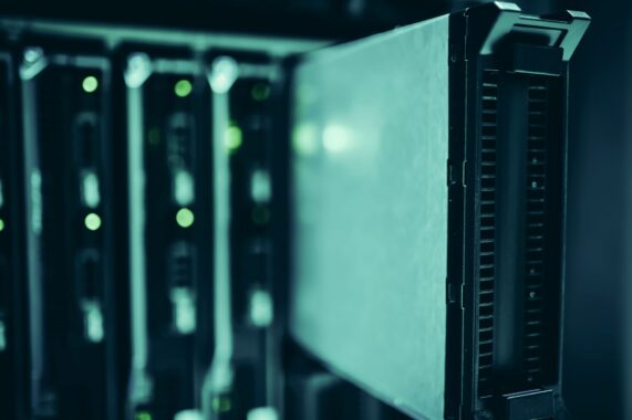
Google announced that it expanded its eighth-generation AI accelerator portfolio on November 9, 2026, with two new systems. TPU 8tx is designed for confidential inference and small-scale training. TPU 8i Max, meanwhile, focuses on workloads that require very large context windows and higher rack density. According to Google, with these additions, 2026 became the first year the company introduced four separate TPU systems.
The company says it has around 100 TPU customers, including frontier labs, trading firms, retailers, and universities. The TPU business covers both Google Cloud infrastructure and deployments in customers’ own data centers.
TPU 8tx protects sensitive data even during processing
TPU 8tx targets regulated institutions and public-sector organizations running frontier or in-house models and autonomous agents alongside sensitive data. With traditional encryption, data can remain encrypted both at rest and in transit, but it still has to be decrypted in memory during computation. The new system aims to keep sensitive data and model weights isolated even during active processing.
The system uses the same silicon as the training-focused TPU 8t, paired with 5th-generation AMD EPYC processor servers and the low-latency Boardfly network developed for real-time reasoning. Google says it delivers up to 2x lower latency compared to TPU 8t, with almost no performance loss.
This combination brings together tasks like model fine-tuning, distilling a large model into a smaller one, and training agents with reinforcement learning on a single system. Private data can stay on the same system without having to be moved across different clusters.
TPU 8i Max focuses on the memory bottleneck
TPU 8i Max is intended for workloads where dozens of agents work simultaneously across an entire software codebase or hours of video. In these kinds of tasks, the bottleneck is not raw compute power but memory bandwidth. Google’s answer is to combine two low-latency TPU 8i chips into a single package.
According to the company, the package delivers 2x the compute power, 2x the on-chip SRAM, and 2x the high-bandwidth memory (HBM) bandwidth compared to TPU 8i. Because the package fits within existing rack dimensions, data centers can deploy more compute per square meter and per watt. The base TPU 8i and 8t were introduced in April 2026 at the Google Cloud Next event; 8i combines 288 GB of HBM with 384 MB of on-chip SRAM.
Not a new chip, but a new system
Google does not see these two launches as the arrival of new base chips. A new chip requires billions of transistors to go through a design and manufacturing cycle that takes years. A system, on the other hand, defines how compute, networking, storage, packaging, and security are brought together around that silicon.
The company’s modular AI Hypercomputer approach treats TPUs, memory, the optical network, and security as configurable building blocks. Google says this makes it possible to deliver custom supercomputers in months rather than years. TPUs have long been co-designed with Google DeepMind, and the company says requests from external organizations also helped shape these two systems. The standout demands were very large context windows and dedicated encryption for regulated workloads.
Source: Unite.AI

Share your experience
Bir sorunun, farklı bir çözümün veya eklemek istediğin bir notun var mı? Giriş yapmadan da yazabilirsin.