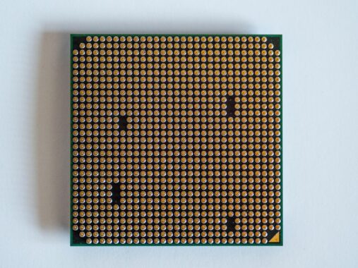
Graphics processors that train AI models, enable autonomous vehicles to perceive their surroundings, and render game worlds actually emerge at the end of a long manufacturing chain that begins with sea sand. A GPU contains more than 100 billion transistors, and these circuits are designed to perform trillions of matrix operations per second. Each link in this chain relies on technology owned by only a handful of companies worldwide.
From Sand to Monocrystalline Silicon
The raw material is silicon obtained from quartz, which is abundant on beaches. However, the material used in chip manufacturing must be extraordinarily pure; not even one foreign atom in a billion may remain. Purified silicon is melted at 1,420 degrees Celsius using the Czochralski method. A flawless seed crystal is dipped into the melt, slowly rotated and pulled upward, eventually forming a single-piece monocrystalline cylinder weighing more than 100 kilograms, known as an ingot.
This cylinder is sliced into disks about 775 micrometers thick using diamond-coated wire saws. The resulting round disks are called silicon wafers. The wafer surfaces are polished using chemical and mechanical abrasion until no microscopic scratches remain.
ASML and Extreme Ultraviolet Lithography
Once the wafer is ready, the next step is to draw circuit patterns onto it. In a modern GPU, transistor gates are 3 to 5 nanometers in size; the width of a human DNA helix is about 2.5 nanometers. The wavelength of visible light is not short enough to draw details this small. At this point, EUV lithography machines made by the Dutch company ASML, each costing more than $300 million, come into play.
Inside the machine, high-powered carbon dioxide lasers fire twice at molten tin droplets falling 50,000 times per second. The tin vaporizes into plasma and emits extreme ultraviolet light with a wavelength of 13.5 nanometers. Because this light is absorbed even in air, the inside of the machine is kept under a deep vacuum, and the world’s smoothest mirrors are used instead of lenses. The pattern is reflected onto the photoresist-coated wafer through these mirrors with a precision of one-millionth of a millimeter.
70 to 100 Layers at TSMC
The chemical areas hit by the light are etched away with acid; then ion implantation, metal deposition, and etching cycles are repeated. The resulting structure is not a single plane but a maze of copper and cobalt wiring with 70 to 100 stacked layers. At TSMC’s fabs in Taiwan, the time from a wafer entering the cleanroom to the completion of all chips can take 3 to 4 months.
CoWoS and HBM Packaging
The wafer is finally cut into individual chips with diamond blades. However, a GPU built for AI is not made from a single piece of silicon. No matter how fast the processor is, if it cannot fetch data from memory in time, it has to wait. The solution is to stack memory chips called HBM on top of one another and connect them with microscopic silicon holes.
In the 2.5D packaging method called CoWoS, pioneered by TSMC, the main compute chip and eight HBM memory blocks are soldered side by side on a silicon interposer at micron-scale distances. This makes data transfers exceeding 8 terabytes per second possible in a single GPU package. This packaging capacity is today a tighter bottleneck in the production of AI chips than silicon speed itself.
Source: WebTuring


Share your experience
Bir sorunun, farklı bir çözümün veya eklemek istediğin bir notun var mı? Giriş yapmadan da yazabilirsin.